S100 Computers

Home S-100 Boards History New Boards Software Boards For Sale
Forum Other Web Sites Quiz Index    
  
An S-100  Z80 Based /Western Digital 2793 Floppy Disk Controller Board
There was a time when a floppy disk was the primary means of storing and exchanging data on an S-100 system.  The original Altair, IMSAI and Cromemco systems used 8" floppy disk drives. Very soon (~1979), 5" drives started to appear in real numbers as well. Early on the hard sectored "Northstar" & "Micropolis" drives were popular. However over time soft sectored based disk systems dominated the market.  This was primarily due to their ease on implementing on an S-100 board using the Western Digital 1771 FDC chip.  This chip was soon replaced by the 1791/1795 chip which could read single and double density soft sectored 8" and 5"  drives.  In the end ,almost every S-100 board manufacture had their own Western Digital DFC board.  Only later did the floppy disk market switch over to the NEC 765 chip based systems -- spurred on initially by its use in the IBM-PC.

Writing an efficient fast FDC "BIOS" for an S-100 8080/Z80 based system was almost a "right of passage" for many experienced S-100 programmers. Bring up  CP/M with a FDC introduced many of us to software programming.  Because the data rate coming in from a double density disk was close to the limit that a 4 MHz (and past that of a 2MHz) Z80 chip could handle, efficient code had to be incorporated in places.

Two basic hardware approaches were used. One involved using a dedicated DMA controller chip that temporally took over the S-100 bus for actual sector reads and writes.  The CompuPro Disk1 would be a good example of this approach. The second utilized a port I/O approach synchronized to the FDC chip's data via wait states placed on the S-100 bus.  The SD Systems Versafloppy FDC boards were one of the first and best example of this latter approach.

With both approaches each new operating system (CPM+,CPM86, CPM68K, MSDOS etc) and/or each new FDC board required essentially a  completely new BIOS be written and debugged.

Since my long term goal is to have a multi-processor Master/Slave S-100 system utilizing not only Z80,8086,80386,68000 etc CPU's but also modern ones like the PIC , ARM or Propeller families, I wanted to construct an S-100 Based FDC board where a minimum software development process would be required for each CPU.

Unlike those early days,  much faster versions of the Z80 now exist. Versions up to 20MHz are available.  This allows one to construct an S-100 board with a completely dedicated Z80 to interface with a WD 179x type chip on one side and the S-100 bus on the other such that ALL interactions with the floppy disk can be reduced to one byte "commands" in the BIOS for each of the above systems.  The board is completely IO mapped (to a block of four IO addresses). No wait states are required -- things are real simple. 

Now many CPUs could be utilized.  Something like a PIC or Propeller CPU would probably be the most elegant. However it turns out something as simple as a dedicated 6MHZ Z80 is quite fast enough to keep up with the data rate to/from a Western Digital FDC chip for even the worst case situation (formatting a disk track in double density).  I opted for the lowly Z80 simply because I have a solid Z80 based BIOS to start from, know the opcodes well and have on hand, the required CPM based assembler linker etc.  Utilizing a more modern/faster CPU will not get you a significantly faster FDC card from the S-100 bus prospective. Data coming/going to the disk is the rate limiting step by far.

As we will see the core of the CPU design is a three chip set of a Z80 CPU and two Zilog PIO's.  Zilog put together this combination a very neat and efficient interrupt driven setup where with just these 3 chips you get four 8 bit I/O ports each with its own strobe and status pin.  Just adding a ROM and a single RAM chip and you have a self contained "computer" on your S-100 board.  What is really nice about all this as well is you can developed and test your software initially in your own S100 system using CP/M and a S-100 FDC board like a Versafloppy.  This is what I did.

As many of you may know the "trick" is designing those old FDC boards was designing the "data separator" circuit to process the raw data coming in from the disk itself.  A number of phase lock loop designs were used and all required some finesse in getting them to work reliably.  A good scope was almost an essential requirement often with a test disk.  Modifying the circuit for single and double density disks was extra!

Over the years Western Digital and others also continued to improve and simplify the requirements of the FDC chip.  The apex (and final) design of the Western Digital 179x design was a 40 pin chip called the Western Digital 2793 chip (WD2793).   This is what the 179x design should have been all along!  It brought the data separator circuit directly on to the chip eliminating the need for the designer to address the issue.  It allowed 5" and 8" drives to be addressed in both single and double density formats using only one (2MHz clock) signal input.  Best of all it was completely compatible in software with the earlier 179x series. An old BIOS written for that chip would immediately run in an WD2793 system.  As we shall see the chip layout design is really simple and clean.  It was for a time a very popular chip being used in for example the Atari computers. It later became second sourced to TI, NEC and others.  Interestingly enough the early chips were rated for 4MHz driven CPU (with no I/O wait states) but every chip I used (WD-two chips,  TI and VTI-2  chips) run rock solid at 6MHz. The WD and VTI chips run at 8MHz.  These are 1982 date stamped chips, BTW.  This was (as we will see below), probably helped by the design of the board. Besides the three 40  pin Zilog chips mentioned above,  the 40 pin WD2793 chip sits next to the Z80 (and RAM & ROM chips).  All are directly connected with no bus buffers etc.

The 6MHz speed is important because at that speed the Z80 is fast enough to get/send data to the WD2793/Floppy disk AND at the same time read the status port of the WD2793 for data synchronization WITHOUT any hardware for wait states or a dedicated DMA controller.  The software becomes very symmetrical clean and simple -- just looking at ports and sending data to those ports.

It becomes a real joy to program for because all the Z80 does is talk to the WD2793 on one side and the S-100 bus and the S-100  bus on the other.  Nothing ever disturbs this process. The code is always in ROM and never changes.  Since the board as we see has 32K of EEPROM space and 32K of RAM there is plenty of room to get fancy.

As an added extra we now have space in ROM to do things a typical S-100 board would not have.   As I said the WD style chips worked (only) on soft sectored disk formats. I this respect they were extremely capable, being capable of addressing almost any sector size, track size and indeed data density.  That's the good news. The bad news is that this lead to a proliferation of different disk formats. Particularly for the 5" disks. Almost no two company 5" disk formats were alike.  This lead to frustration in exchanging disks and indeed in selling software on disks.  One of the neat aspects of having a dedicated Z80 on board is now we can write software (in EEPROM) that completely (and transparently the S-100 side) takes care of understanding the actual disk format on the disk.  As far as the S-100 system is concerned its just a disk with a certain sector size, sectors/track and tracks/side.

One other challenge with FDC boards is what to do when the system hangs. If for example a user puts in a wrong disk format, or worse an unformatted disk and tries to read it.  Many FDC boards hang because the WD chip is confused or the S-100 bus itself is locked in a continuous wait state.  On this ZFDC board from the S-100 side BIOS one can reset the ZFDC board Z80/WD2793 hardware if the board times out in such situations. 

It is also "Nice" to know exactly where the head is on a disk at all times. The board has 5 LED HEX displays that display the current disk number, current track and current sector as well as bi-color (red/green) LEDs for the current disk size (8"/5") density (SD/DD) and side being read (Side A/Side B).

All the above said, it turns out that arriving at a final design for the board and developing the software took way longer than I expected. As Andrew will attest to, we went through 18 modifications of the original Prototype board (shown here), to arrive at a second prototype board, shown below.  Here is a schematic of this second board.
 
  
ZFDC Prototype1

  
Likewise the software development was quite time consuming. There are two components:-

ZFDC.Z80          
This is the EPROM based software that controls every aspect of the board. On the S-100 side the board appears as one 8 bit output port and a 2 bit input status port as well as an 8 bit input port with a 1 bit output status port.  This software can be seen here and downloaded here. (See bottom of page for the most up to date versions).

ZDFCDIAG.Z80
This is a CPM based program that can be used to test the board. Near the beginning are simple "Callable BIOS routines" that can be spliced directly into any CPM BIOS.  It can be seen here and downloaded here. (See bottom of page for the most up to date versions).

Both pieces of software are described in more detail below, but in a nutshell the board works by receiving 8 bit "commands" from the S-100 system (followed by none, one or more parameter bytes) for things like:- select a disk, track, sector etc  and read/write a sector or track.  All hardware decisions, time delays, status checks etc  are handled by the ZFDC board.  For example with one command (a one byte command and, an in this special case a confirmation byte) you can format a complete disk track to any one of (currently) 14 formats.    All the Z80 source code is commented on in detail. I will be delighted to add improvements, more formats etc. from others.


Understanding the Western Digital WD2793 FDC chip

WD2793 Hardware
Like the earlier 1791/1795 chips the WD2793 consists of a 40 pin chip with many of the same data and control lines as the earlier 179x series. To understand the ZFDC board you really have to become familiar with this chip.  The complete data sheet can be seen here. You should read this data sheet in detail to understand much of what I have below.

Let us first look briefly at the function of the 40 pins:-

  Pinout 1   WD2793 Chip
   
  Pinout 2
     
  Pinout 4   WD2793 Raw Chip

Most of the pins are fairly straightforward and should need no further discussion.  Pins #26 and #33 as we shall see, do need to be adjusted, but Western Digital (by this stage) made it easy to do with a special test pin (#22).  The one complication in any system is if you intend to use the chip with both 8" and 5" drives mixed together.  Because the data rate of a 5" drive is half that of an 8" drive the clock frequency has to be divided in two.  Pin #25 is set aside for this use.

One very important control pin is  INTRQ (#39). This pin pulses high (very briefly) when every a command is completed.  We will gate the output of this pin going to the NMI pin of the Z80 such that (if desired) the Z80 will experience a NMI interrupt whenever the  WD2793 completes its current command (seek, read a sector, format a track etc.).  This is a very convenient and efficient way to synchronize the two chips. 

WD2793 Software
All Western Digital FDC chips have at their base port a key "status" port that continuously displays important information about the chips actions and results.  This is reflected in a series of bit flags. The actual meaning of these bits changes depending on what the chip has being doing.  Here is a summary of the bit flags for the most common uses:-

Status register

The challenge with any disk controller is matching the data rate of the stream of data bits coming in from the disk surface with the capability of a CPU's ability to place the corresponding bytes in memory AND at the same time decide when the job is done.  In the early S-100 days when only 4MHz Z80's were available, the Z80 simply could not keep up.  In other words the Z80 was not fast enough to continuously monitor the status register status bits AND at the same time take data from the data port  and place it in RAM -- particularly in double density modes.  Two basic ways around this were used. One was to use a dedicated DMA controller on board (which was fast enough) -- but this sometimes caused conflicts with other (pre-IEEE696) S-100 boards.  The other simply took account of the fact that IF there are no errors, one knows exactly how many bytes to expect (or send) and you can lock the data rate of the FDC to that of the Z80 utilizing the Z80's block I/O instructions and inserting CPU wait states during each bytes transfer at  the same time counting the total number of bytes processed.


Fortunately utilizing today's 6MHz Z80's (or faster) you don't have to use these round about approaches.  The Z80 can simply input individual disk bytes AND at the same time look at the WD2793 status port to see when the next byte is available (bit 1, the DRQ bit goes high).  That said things are still very tight.  You really have to watch your clock cycles.  To input a sector here is the key code I use:-

READ_SECTOR:
                    LD      DE, Sector_Size
                    LD      HL, DMA_Address
                    LD      C, Data_Port             ;Utilize the special Z80 op-code to use the [C] register to address a port           
 CHK_STAT:  IN      A, (WD2793_Status)
                    RRA            
                    RRA
                    JR      NC, CHK_STAT          ;Very fast way to check the DRQ status bit
                    INI                                     ;Very fast way to input data from [C] port ->[HL++]
                    LD      A, E
                    OR     A, D
                    JR      NZ, CHK_STAT           ;Continue until [DE] is zero


Using this very efficient code a 6MHz Z80 is well able to keep its head above water!  BTW, a faster CPU makes no difference and indeed may be unreliable since you are way outside the specs of the WD2793 chip.  Code like this in fact can be utilized to read or deposit a whole track on a disk.

All of the above is perfectly fine so long as there are no errors. However if for some reason the WD2793 comes up short in getting bytes from a sector (a wrong formatted disk was used for example), the system will hang.  There is not enough time to incorporate a software timeout counter in the loop.

  
What we do, in hardware, is trigger a 74LS123 pulse generator. Before we read or write a sector we trigger/activate the 74LS123 (Watch-Dog Timer).  IF a sector is not read before the timer times out, it triggers a NMI interrupt on the Z80 which then causes the Z80 to brake out of the above loop and act accordingly. If the sector is read/written properly in time it turns off the watchdog timer.

As an extra safety net, the Z80 NMI line is also triggered by the INTRQ pin of the WD2793 pin which always pulses when an WD2793 operation is complete. I have the hardware where this line too can be activated to trigger an NMI instruction.  The software is a little tricky but is documented in ZFDC.Z80 above. 

The above arrangement makes for a very reliable WD2793 arrangement to seek, read/write sectors or tracks etc.  There are no wait states, no DMA controllers or inserted HALT opcodes. (A special thanks to Chuck Guzis for helping me figure all this out).

The ZFDC Board Software.
The basic concept in the ZFDC EPROM software is quite simple. After checking RAM, initializing the PIO's and initializing various software flags in RAM, the Z80 does nothing more than look at the input from the S-100 data port PIO for a one byte "command". Execute that command (which may, or may not, involve further input bytes) and send the information to the WD2793 FDC chip.  The result of that command is then sent back to the S-100 system via the boards second PIO output port. Normally the S-100 side will receive a "NO_ERRORS" byte followed by varying amounts of extra bytes of data. The whole process is repeated indefinitely.  If for whatever reason there is a problem, the S-100 side of things will not receive a "NO_ERRORS" byte but a one of about 50 error codes. 

Here is a list of the major commands the ZFDC board expects to receive:-

CMD_PIO_TEST      EQU   0H          ;Simple loop hardware test of PIO #1 Ports
CMD_MONITOR       EQU   1H          ;Jump to internal ZFDC monitor.
CMD_SHOW_SIGNON   EQU   2H          ;Sector Display TIL's as a hardware test
CMD_RESET_2793    EQU   3H          ;Reset the WD2793 chip and Board software
 
CMD_SELECT_DRIVE  EQU   4H          ;This will select a specified drive and disk format
CMD_GET_DRIVE     EQU   5H          ;Return the current Disk number (0,1,2,3)
CMD_GET_FORMAT    EQU   6H          ;Return the current Disk Parameter Format Table number
CMD_SET_TRACK     EQU   7H          ;This will set head request to a specified track
CMD_SET_SIDE      EQU   8H          ;This will set side request to a specified side
CMD_SET_SECTOR    EQU   9H          ;This will set sector request to a specified sector
 
CMD_SET_HOME      EQU   0AH         ;This will set head request to Track 0 of CURRENT drive
CMD_STEP_IN       EQU   0BH         ;Step head in one track of CURRENT drive
CMD_STEP_OUT      EQU   0CH         ;Step head out one track of CURRENT drive
CMD_SEEK_NV       EQU   0DH         ;Seek to track with NO verify of CURRENT drive
 
CMD_SEEK_TRACK    EQU   0EH         ;Seek to CURRENT track (with verify)
CMD_GET_TRACK_ID  EQU   0FH         ;Read the CURRENT TRACK ID
 
CMD_READ_SECTOR   EQU   10H         ;Read data from the CURRENT sector.
CMD_WRITE_SECTOR  EQU   11H         ;Write data to the CURRENT sector.
 
CMD_GET_WD_TRACK  EQU   12H         ;Get the WD2793 Track register value
CMD_GET_WD_SECTOR EQU   13H         ;Get the WD2793 Sector register value
CMD_GET_WD_STATUS EQU   14H         ;Get the WD2793 Status register value
 
CMD_TRACK_DUMP    EQU   15H         ;Dump complete CURRENT track to the S-100 system
CMD_FORMAT_DISK   EQU   16H         ;Format the disk in the of the CURRENT drive
 
CMD_SET_DEBUG_ON  EQU   17H         ;Turn on Debug display mode
CMD_SET_DEBUG_OFF EQU   18H         ;Turn off Debug display mode
CMD_RAM_DUMP      EQU   19H         ;Data dump to S-100 system of all memory variables/flags
CMD_ABORT         EQU   20H         ;Generalized Abort of the current process command.

WD2793 Commands
Exactly like the earlier 1791/1795 chips the WD2793 contains five 8 bit registers which completely control all the chips functions. They are:-

Data Register.         This is the register to/from which sector byte by byte data is obtained.

Track Register.       
The require disk track is placed in this register. Upon a track seek (with verify) the new track can be read from here

Sector Register.      
The require sector to be read/written to  is placed in this register.

Command Register 
This is the most important register it determines what next the chip will do.

Status Register       
This register contains various flag bits to describe command success or errors.
  
 
Tracks on a disk are laid down in the format:-
 
Track header...gap...(Track/Sector ID..gap..Data..gap) x N times, ...End of Track

The Track/Sector ID consists of 6 bytes:-

Track#,  Side (0 or 1), Sector#, Sector Size flag (,1,2,3 or 4) , and a 2 byte CRC check.

The command register accepts 11 different commands with very precise bit patterns.  They are summarized in this table.

WD2793 Commands

First you will notice that the commands are grouped into 4 groups. 

The
Type I commands control the head movement. Bits 0 and 1 determine how fast the head will move from track to track. For most modern drives the maximum speed so these bits are 0,0.  The V bit determines if the chip will verify if it is on the correct track after the head to track movement is complete. Normally a 1 but for disk formatting it is set to 0. The h bit determines if the head is to be lowered on to the disk before or after the command function is complete.
 
The
Type II commands are clearly the most important (but the most complex).  Bit 0 of a Write sector 'a0' has to do with disk formatting and need not concern us here and is set to 0.
 
F1 is another story. This bit simply determines if the chip is to check if the active head is reading from the requested side of the disk. If 0 the WD2793 chip skips this side check. If 1 it checks that the active head is really on the requested side. The side of the disk is contained in the Track/Sector ID field. The second byte of this field is 0 for side A (or a single sided disk). It is 1 for side B.
 
The E bit determines if there is to be a slight time delay (15 ms) in setting the chip's busy flag after lowering the head.
  
F2 on a WD2793 chip is relevant if F1 was set to 1 (enable side compare).  If it is 0 the sector side field must also be 0 (Side A). If it is 1 then the sector side field must also be 1 (Side B).
 
Finally the m bit allows you to read/write contiguous sectors on a track. Very fast, but unfortunately difficult to incorporate in CPM BIOS code because multiple sectors often are on different tracks.
  
The
Type III command either reads the above track/sector ID field or a whole track. The write track command is primarily for disk formatting.
  
The
Type IV command, force interrupt command is to pull the chip out of a lockup situation. It's basically a chip reset command.


To understand better how to control the chip take a look here at a CP/M diagnostic program in Z80 code for the ZFDC Board I wrote called Z
FDCDIAG.COM. The source code for this diagnostic program can be seen here (ZFDCDIAG.Z80) and downloaded here (ZFDCDIAG.COM).  Here is a picture of the ZFDCDIAG.COM.

ZFDCDIAG

Programming this chip was a lot of fun and quite rewarding in allowing me to write a fast and efficient CPM BIOS.  Most of the commands are self explanatory. It is menu driven. Each command requires a two digit HEX number followed by a CR.

Menu item 17 turns on/off a detail display of actual sector data on the CRT. Useful if you are checking out large format sectors. 

Menu item 19 causes the ZFDC board to jump to its own internal ZAPPLE like monitor from which you can do all the usual things like display RAM, I/O directly to ports etc. Useful for debugging. 

Menu item 1E switches the HEX display from displaying the current Track, Sector, Drive to a mode in which it displays the current command it is working on and the LAST error code (if any) it sent back to the S-100 system. Again very useful for debugging but not normally used. 

Menu item 1D displays a complete data dump to the S-100 of all critical RAM stored variables the Z80 and WD2793 are using for all four possible drives A:,B:,C: D: as well as other critical things such as the stack location etc.

Menu item 11 displays on the S-100 CRT a data dump of a complete track from the disk -- useful for formatting issues etc.

However most of the time if you use this program you will only use menu item 00.  This brings up a sub-menu that allows you to format a disk -- either the whole disk or the data area on the disk.  As I said above the complication here is that there are many different formats. And while you would normally use this board with either an 8" Single density IBM 128 byte 26/sectors/track disk or a double density MS-DOS formatted disk, you can use (currently) 12 other disk formats. 

The disk formats available are:-
8" SDSS, 26 X 128 Byte Sectors, (IBM 3740 Format).
8" DDSS, 50 X 128 Byte Sectors, (SD_Systems Format).
8" DDDS, 26 X 256 Byte Sectors, (IBM System 34 Format)
8" DDDS, 15 X 512 Byte Sectors.
8" DDSS, 8 X 1024 Byte Sectors.
8" DDDS, 8 X 1024 Byte Sectors.
5" SDSS, 17 X 128 Byte Sectors, (SD-Systems Format).
5" DDSS, 28 X 128 Byte Sectors, (SD-Systems Format).
5" DDDS, 8 X 512 Byte Sectors,  (IBM PC CPM-86 format).
5" DDDS, 9 X 512 Byte Sectors,  (DEC VT180 format).
5" DDDS, 16 X 256 Byte Sectors, (TOSHIBA T-100 format).
5" SDDS, 18 X 128 Byte Sectors, (CROMEMCO CDOS Format).
5" DDDS, 10 X 512 Byte Sectors, (CROMEMCO CDOS/CPM Format).
5" SDDS, 10 X 512 Byte Sectors, (EPSON QX-10 Format).
5" DDDS, 5 X 1024 Byte Sectors, (MORROW MD3 format).
5" DDDS, 8 X 512 Byte Sectors,  (ZENITH Z-100 format).
5" DDDS, 10 X 512 Byte Sectors, (SUPERBRAIN QD format).
5" DDDS, 8 X 512 Byte Sectors,  (IBMPC MSDOS 1.1 format).
5" DDSS, 10 X 512 Byte Sectors, (TRS-80 MOD-III format).

As I also explained above, this formatting is completely transparent to the S-100  system side of things. In fact in a multitask/user system the S-100 side of things can go off and do something else.

Many more formats can be very easily added because formatting is done completely based on a 21 byte "Format Parameter Table" for each disk format.  Less than 16K of the 32K EEPROM is currently used.  Here is an example of the format table for an 8" IBM Single density disk:-
;           8" SINGLE DENSITY DRIVE VARIABLES (IBM 3740 Format)
STD8IBM:
            DB      00011000B     ;Disk HW_BYTE (SDSS)
            DB      26+1          ;SECTORS PER TRACK (+1)
            DB      77            ;TRACKS PER SIDE
            DB      40            ;HEADER GAP
            DB      6             ;GAP 1 (0's)
            DB      11            ;GAP 2 (FF's)
            DB      27            ;GAP 3 (FF's)
            DB      247           ;GAP 4 (FF's)
            DB      1             ;GAPR (Flag for multiple repeats of GAP4)
            DB      0             ;128 Bytes/sec
            DB      0FFH          ;GAP Format fill character
            DB      0E5H          ;Data area fill character
            DB      0H            ;No special post format
            DW      SKEW_IBM      ;Location of this disks sector skew table
            DB      01H           ;Each format will have a unique number.
            DB      2             ;Tracks set aside for operating system (e.g. CPM 2)
            DW      128           ;128 Bytes/sec
            DW      13F0H         ;Size in bytes of 1 formatted track
            DB      '8" SDSS, 26 X 128 Byte Sectors (IBM 3740 Format)',0
SKEW_IBM:
            DB      1H,2H,3H,4H,5H,6H,7H,8H,9H,0AH,0BH,0CH,0DH,0EH,0FH
            DB      10H,11H,12H,13H,14H,15H,16H,17H,18H,19H,1AH

With these disk format tables you should be able to easily read old 8" and 5" disk formats and if need be send to others (if need be in a different format).


A Second Prototype ZFDC Board
Based on working with the above prototype board for a few weeks, I improved the design and designed a second board.  There were many small additions and improvements. More LED's to let you know what is going on. Also better status signals being passed back to the S-100 bus for the same reason.  Also added was the capability to trigger the Z80's NMI line based on a 74LS123 timer or triggering by the WD2793's INTRQ line.  Here is a picture of this board:-
 
V2 Prototype
 
With this board the software started to behave very reliably. There were unfortunately still a few minor improvements necessary.  In particular it became clear that if one wanted to have both 8" and 5" (or presumably 3"), floppy disks together attached to the board it was necessary to have separate 74LS06 output drivers for both ribbon cable connectors.   Also I added circuitry such that the timer and/or WD2793 INTRQ lines could separately and independently trigger the Z80's NMI line.   The board utilizes a 2MHz clock generator for the WD2793 chip and a 6MHz clock generator for the Z80. 
 
As I said above, the second prototype board behaved quite reliably and allowed me to write software to interface multiple disk drive systems/formats. By way of example I wrote a simple CPM3 BIOS for two 8" drives and one 5" drive. The source code for this BIOS can be seen here, and the code can be downloaded from here

A few things about this BIOS. First you can see that a board like this lends itself nicely to working with CPM3.  CPM3's BIOS compresses all disk interactions into just four calls:-

Disk Initialization,  Disk Login, Sector Read and Sector Write.

That's it.   On top of that it takes care of all disk buffering, sector sizes etc.   This makes interfacing the BIOS to the ZFDC board extremely easy.  Here for example is the core code to CPM3 write a sector routine:-
 

  WRITE$SECTOR:
       MVI    C,CMD$SET$TRACK
       CALL   S100OUT
       LDA    @TRK
       MOV    C,A
       CALL   S100OUT                 ;Send Selected track
       CALL   WAIT$FOR$ACK            ;Return Z (and NO$ERRORS$FLAG in [A]), or NZ with error # in [A]
       JRNZ   WRITE$ERROR
 
       MVI    C,CMD$SET$SECTOR         ;Sector # to side A (or for DS disks also side B)
       CALL   S100OUT
       LDA    @SECT
       INR    A                        ;Disk sectors 1...MAXSEC
       MOV    C,A
       CALL   S100OUT                  ;Send Selected sector HEX number
       CALL   WAIT$FOR$ACK             ;Return Z (and NO$ERRORS$FLAG in [A]), or NZ with error # in [A]
       JRNZ   WRITE$ERROR
 
       MVI    C,CMD$SEEK$TRACK   
       CALL   S100OUT
       CALL   WAIT$FOR$ACK             ;Return Z (and NO$ERRORS$FLAG in [A]), or NZ with error # in [A]
       JRNZ   WRITE$ERROR
      
       MVI    C,CMD$WRITE$SECTOR       ;Now send the Write Sector Command

       CALL   S100OUT                
       CALL   WAIT$FOR$ACK             ;Wait for NO$ERRORS$FLAG to come back
       JRNZ   WRITE$ERROR
      
                              
       LHLD    @DMA                    ;Load up the DMA address
       LDED   SECTOR$BYTE$COUNT        ;and byte count of bytes to be sent (128,256,512 or 1024)
      
       JMP    ADJ$BANK1
       CSEG
;=======================================
ADJ$BANK1:
       LDA    @CBNK
       PUSH   PSW
       LDA    @DBNK                     ;Point to the databank where the data has to come from
       CALL   ?BNKSL
      
WR$SEC:MVI    B,0FFH                    ;Put in a timeout count (Loop for status read at most 256 times)
WR$SEC1:DJNZ  WR$SEC2

        POP    PSW
                      ;Need to get back to DSEG bank!
        CALL   ?BNKSL
        MVI    A,TIMEOUT$ERROR          ;Send Timeout error
 
       JMP    WRITE$ERROR              
                                        ;Note we cannot use S100OUT here since we are no longer in the DSEG bank
WR$SEC2:IN    S100$STATUS$B             ;Send data to ZFDC output (arrive with byte to be sent in M)
       BIT    DIRECTION$BIT,A           ;Is ZFDC in input mode, if not wait
       JRNZ   WR$SEC1
       BIT    DATA$OUT$RDY,A            ;Has previous (if any) character been read.
       JRZ    WR$SEC1                   ;Z if not yet ready
      
       MOV    A,M                       ;Get the byte
       OUT    S100$DATA$B               ;Send it
       INX    H                         ;[HL++] for [DE--] bytes in sector
       DCX    D
       MOV    A,E
       ORA    D
       JRNZ   WR$SEC
 
       POP    PSW
       CALL   ?BNKSL                    ;Back to the original databank
       JMP    CHECK$WR                  ;Get back to DSEG
;=======================================
       DSEG
 
CHECK$WR:
       CALL   WAIT$FOR$ACK               ;Return Z (and NO$ERRORS$FLAG in [A]), or NZ with error # in [A]
       JRNZ   WRITE$ERROR
       RET
 
WRITE$ERROR:
       LXI    H,FLOPPY$WRITE$ERR         ;"Sector Read Error"
       CALL   GET$ERROR$STRING           ;Get Error String from ZFDC Board
       JP     COMMON$RW$ERROR 


As you can see the code is really nothing more than a few calls to the ZFDC board.  Once setup, the board will send the block of data to the requested sector on the disk.   Now what is nice about all this is that,  first, if you decide to use a different disk format you just let the ZFDC board know with a single command (Typically at CPM Boot time, but more elaborate BIOS'es can do so on the fly).   Probably more important however,  when we go to utilize other CPU's  (CPM86, MSDOS, CPM-68K etc), it's a very 
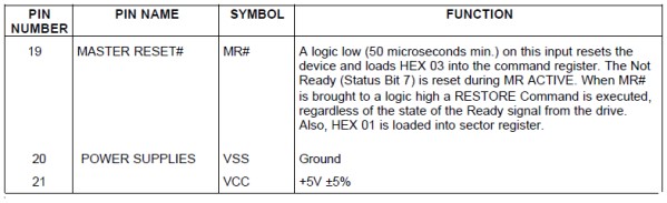
simple rewrite to do a FDC BIOS/Device driver for that system.

A 
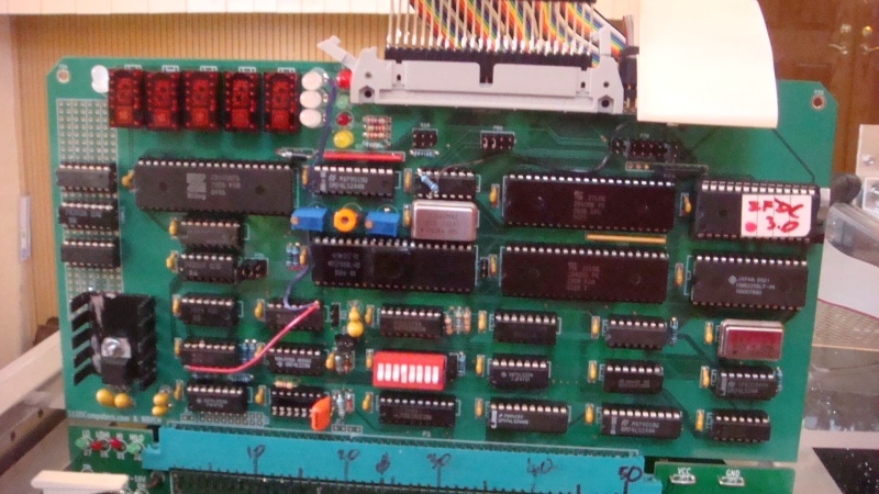
Third Prototype ZFDC Board
Based on working with the above second prototype board for a few weeks, I improved the design and with Andrews help designed a third prototype board.  Again there were many small additions and improvements. Still more LED's to let you know what is going on. Also better status signals being passed back to the S-100 bus for the same reason.  Also added was the capability to trigger the Z80's NMI line based on a triggering by only the WD2793's INTRQ line.   The DRQ and timer circuit described above in the version 2 of the board were no longer needed.  Now the software on both the ZFDC and S-100 side check for hang-ups. This is a more flexible and reliable arrangement.

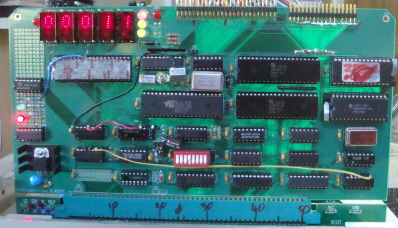
Here is a picture of this third board:-

V3 Board

The schematic of this board at first looks a bit overwhelming, but when you brake it down to its components its fairly easy to understand.   Much of the complexity has to do with the fact that I have split out the ribbon cable connectors for 8" and 5"/3" drives so that each has their own separate jumpers and drivers.   I found that terminating the drives all linked to one connector interface just did not yield reliable (5" drive) data.   Not helping was the diversity of pin designations found amongst 5" & (particularly) 3" drives.

Overall Schematic layout

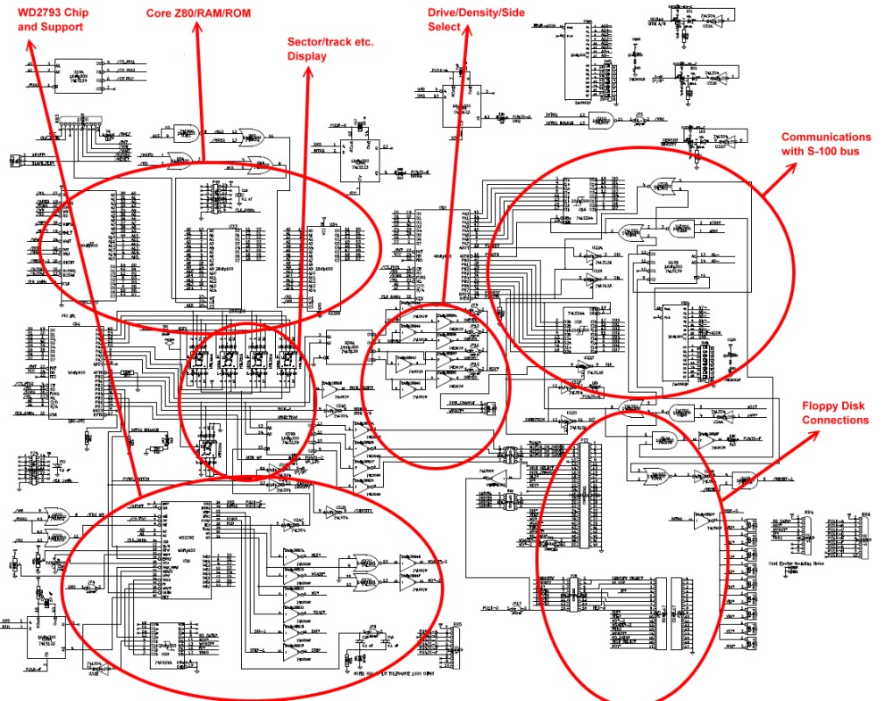
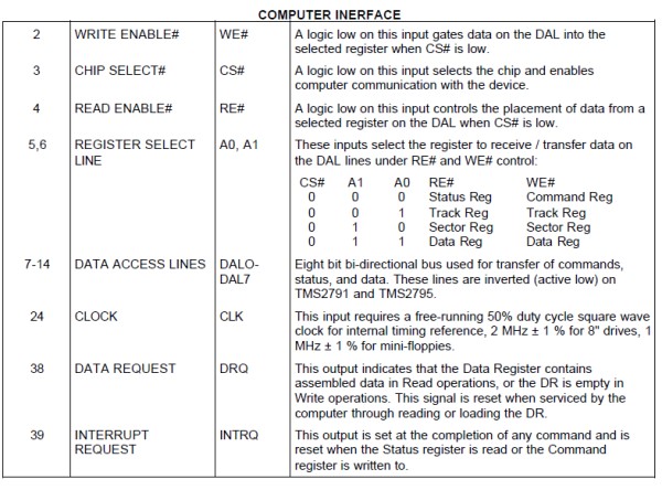
Let us look at each section in turn. The most critical actually turns out to be the interface between the S-100 bus and the ZFDC board internals. All data communications takes place through PIO#1 on the board. However it is necessary to also provide the S-100 bus side with bit flags to know if the ZFDC is ready to receive a command or data and likewise for the ZFDC board to let the S-100 bus side know it is busy or has data available. Complicating things is the fact that data to/from this PIO is interrupt driven in software. Here is a more enlarged map of this region:-

PIO#1

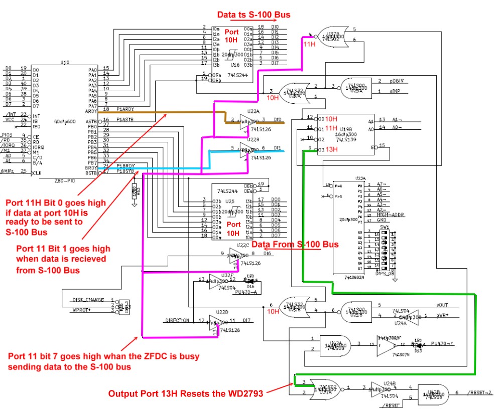
You will also note we have a third port (configured as 13H) which allows the S-100 bus to completely reset the WD2793 chip if the ZFDC board is hung or not responding. This clearly is only used in a drastic situation -- such as the board trying to read an unformatted disk etc.

The second PIO chip on the board controls the floppy disk selection and configuration pins. Here is a map of this region in more detail:-

PIO#2

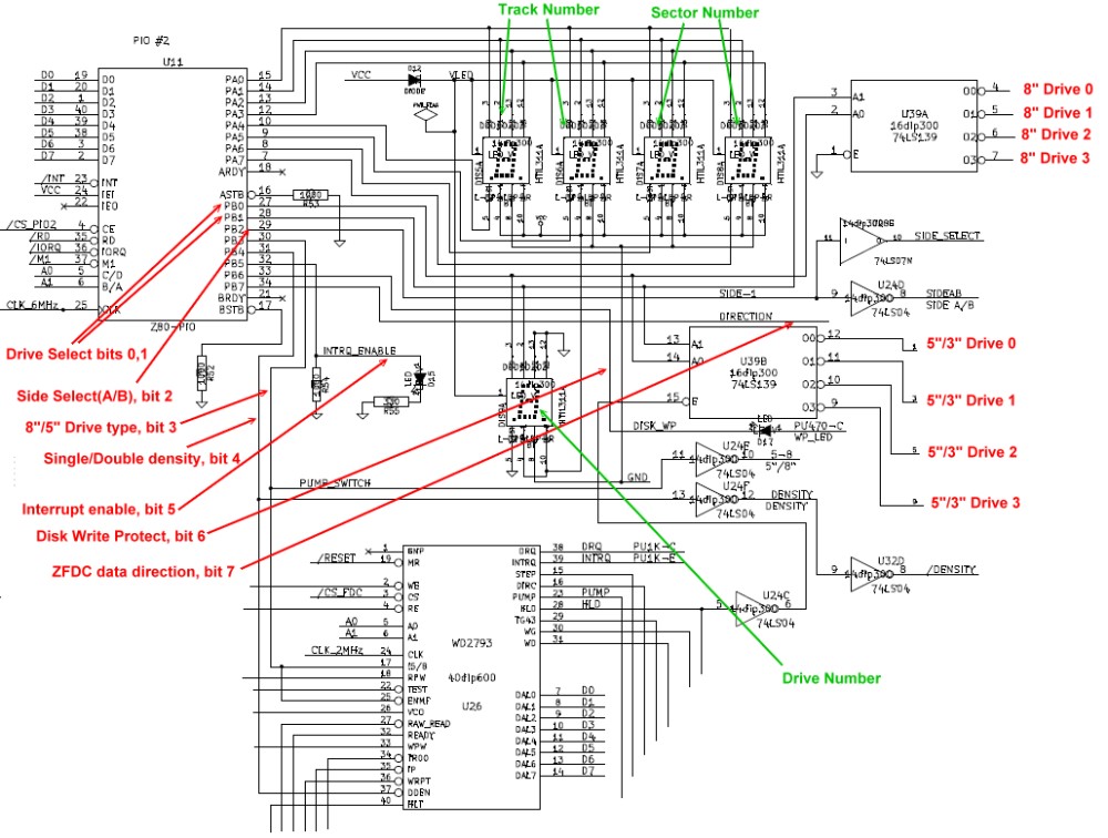
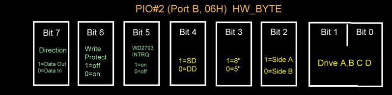
The second dual parallel port PIO (U11) has two functions. The first port, (port A), is completely devoted to displaying the current WD2793 selected disk track and sector. The second port, (port B), is a bit more complex. The lowest two bits (0 & 1) select the current floppy disk in hardware. A maximum of 4 disk drives are allowed.  The two lines are de-multiplexed into 4 drive select lines by the two 74LS139's. U39A is for 8" drives, U39B is for the 5" & 3" drives. Bit 2 selects the A or B side of the selected disk. The WD2793 can work with 5" or 8" (& 3")  disks in terms of data rate.   However the input clock frequency needs to be adjusted. This is done via pins 17 and 25 of the WD2793.  Bit 3 controls this selection, it is high for 8" disks.

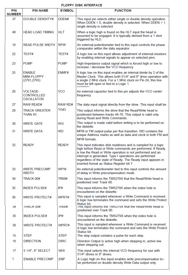
The WD2793 FDC can work with single and double density disks. This is done with pin 37. This is set with bit 4 which is high for single density.

Bit 5 allows the WD2793 INTRQ (pin 39) to trigger an NMI interrupt to the boards Z80.  The WD2793 triggers the INTRQ line when each chip command is completed. This allows the software to be efficiently interrupt driven for things like sector reads and writes   -- (See the ZFDC.Z80 software).

Bit 6 flags whether the current disk is write protected.

Finally bit 7 provides a flag bit to essentially let the S-100 side of things know the ZFDC Z80 is still busy and not to send another command yet.


LED's
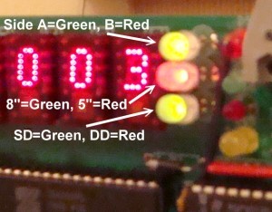
Besides the HEX displays that show the currently selected Drive, Track and Sector, there are three dual colored (Red/Green) LEDs.  These show the currently selected drive size 5"/8", the current selected disk density (SD/DD) and the correctly selected disk side A or B.

For a Single density, 8", Side A, disk all three LED will be green.

By looking at the HEX displays and these three dual colored LED's you can easily check the status of what the WD2793 FDC chip is expecting to see.  In particular as you format different disks always make sure the LED colors match with what you would expect. 

BTW,  when you assemble the board make sure you have the LED's inserted the right way around. Either test each pin for color off the board or go to the board's monitor (menu # 19) and output the appropriate bits to port 06H and check for the correct Red or Green color before you solder the LED in place.

The above port bits are the first entry in each "Disk Parameters Table" in the software that drives the ZFDC onboard Z80.  It is called throughout the software "HW_BYTE".  Each disk format table needs to have this byte carefully set up. Note, in the tables themselves the high 3 bits are always 0's. Here again is a summary of the bit information:-

HW_BYTE Bits 


For the core Z80 CPU itself there is just a single static RAM chip and an EEPROM chip.

Z80 Section

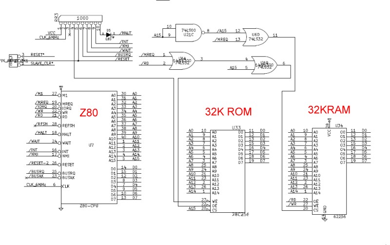
The only addressing circuitry used is address line A15 for addressing EPROM (low) or RAM (High).   These three 40 pin chips along with the two 40 pin PIO's supply the complete onboard "computer" with its four 8 bit input and output ports (with handshaking).  The Z80 halt line is brought out to an LED indicator to test/debug the board during construction.  With just the above circuit (+6MHZ clock) and an EPROM filled with 76's,  the HALT LED should light up for initial testing.  

Since the Z80 runs at 6MHz, only Zilog Z80B parts should be used. These are rated for 6MHz. However I have found at least for the PIO's that older Zilog PIO's work fine.  As explained above, the Z80 cannot keep up with the WD2793 data rate (particularly in DD modes) at 4MHz.  I have actually run these Z80B's at 8MHz with no difficulties what so ever!

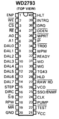
The WD2793 related circuit is fairly straightforward. All chip to disk output lines go through open collector 74LS06's. Critical input lines come back through the Schmitt triggered 74LS244's.   Here is a diagram of this region of the board:-

WD2793 Circuit

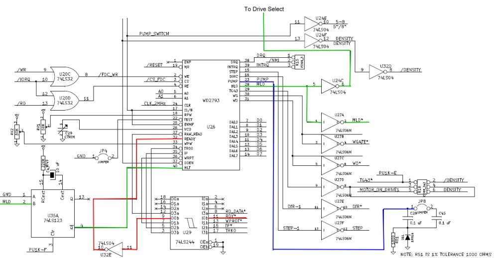
The test (pin 22), RPW (pin 18) and VCO (pin 26) must be adjusted to get the best data/clock separation for your particular setup. I explained below how to do this.  The 50K pot attached to pin 33 (WPW) is used to adjust the "write pre-compensate" on some of the very early 8" drives.  Most later drives take care of this themselves on the drive. If your drive need this adjusted see the WD spec sheet  and/or your drive manual. Failing that,  just set the ZFDCDIAG.Z80 program to repeatedly read/write sectors and tweak the RV2 pot settings by hand until you get no errors.

One pin I was worried about was the "pump" pin (pin23). Input from this pin comes from a resistor/capacitor circuit that controllers the voltage controlled oscillator (VCO) within the WD2793 chip.  Western digital had 0.1uF for 8" drives and 0.2uF for 5" drives. originally I had an analogue switch for each input depending on the drive being accessed.   It seems not to be critical. I use 0.1uF for both drive types. However if you are mainly using 5" drives then install jumper JP8.

The Head Load pin (pin 28) serves two functions. First it AND'ed with each of the drive select pins so that the head is only loaded on the currently selected drive, however it also triggers the 74LS123 (U35A) so that the WD2793 is delayed a little (via the HLT pin 40) to allow the head to settle down before actually reading or writing data.

Here is a short video demonstrating this board in action and a brief display of some of the ZFDCDIAG menu items.


A Production S-100 Board
After 3 prototypes, Andrew Lynch at N8VEM (see here) and I felt we have the board the way we want it! Realizing that a number of people might want to utilize a board like this,  we have  did our first run of a commercial quality board. Here is a picture of the board:-
Final ZFDC board


This is the same as the board above V3 prototype (with some minor changes), for example with Gold plated edge connectors i.e. a "proper" commercial type S-100 board.  If you want one please let Andrew know ASAP. They will be about ~$20 each while supplies last. As always, you get your own parts, no hand holding or manual. (Neither Andrew or I are a commercial venture. We do this along with a group of other people, just for fun!).  Please also note FDC boards are more difficult than most S-100 boards to get working, this should probably not be the first S-100 board you build!

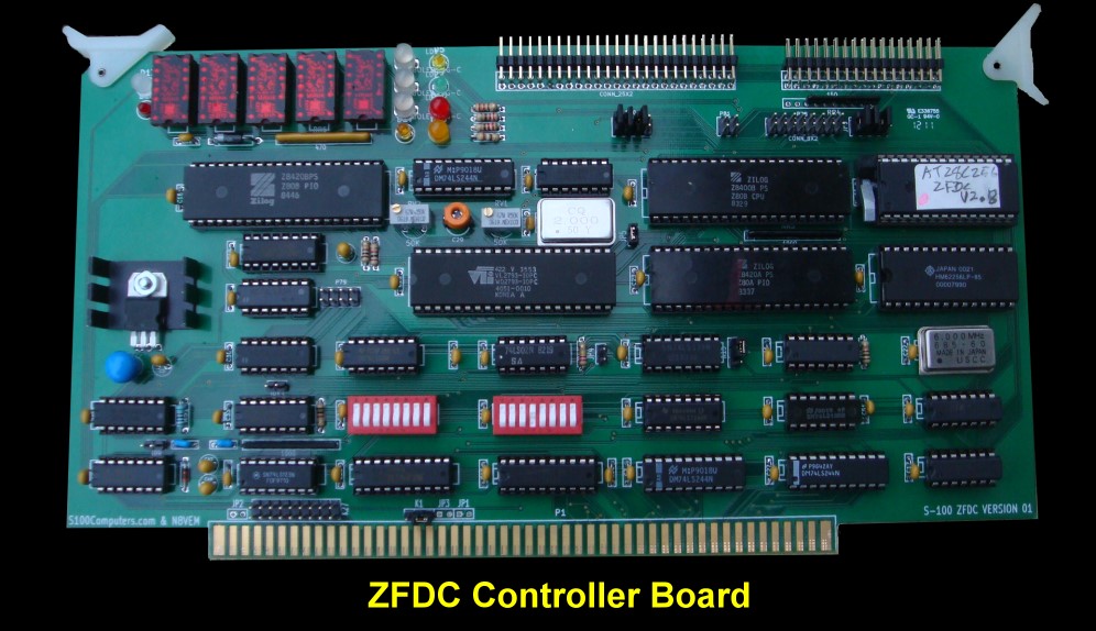
That said, the board is a real joy to work with. Because the BIOS command control is so simple, writing disk drivers for CPM+, CPM86, DOS etc is real easy. As we develop 16 bit S-100 boards we will try and bring this board along with these systems. 

Finally I would like to ask others to provide more extensive software for the board.  I have written a fairly well documented on board Monitor/BIOS, a menu driven CPM based diagnostic program and a separate CPM based disk format program. Additions, improvements etc. are welcome.

I have written both  banked and non-banked versions of CPM3 for this FDC board. It is extensively written up in the software section of this site. Please click here for more information.


Building Board - Step by Step Instructions.

First inspect the board for scratches or cut traces.   Insert all IC sockets, Caps, resistors, the two clock generators (2MHz & 6MHz), resistor networks, the voltage regulator and jumper pins.   I like to solder clock generators directly to the board. If you do use a socket be sure the thin wires make good contact and/or use the special sockets for these "chips". Also make sure to position pin 1 correctly. Take care to get the polarity of caps correct. The square pad is the positive side. Also note that the resistor network RR4 has pin 1 on the right hand side.  Test the empty board for +5 volts on all the empty IC sockets.

Install Jumper K1 (for board reset, bottom of board) to 2-3 position. Install IC's U21 (74LS00),  U23 & U45 (74LS682), U42 (74LS08),  U20 (74LS32),  U24 (74LS04),  U32 (74LS04),  U28 (74LS07)  U37 (74LS02) and U19 (74LS139).  Next install the 8 position dip switches SW1 & SW2.  We will use S-100 I/O ports 10-13H so all switches are close except switch 5 (counting right to left). Here is a picture:-

Dip Switches

Go to your monitor and at 0H in RAM enter

DB, 10, C3, 00, 00

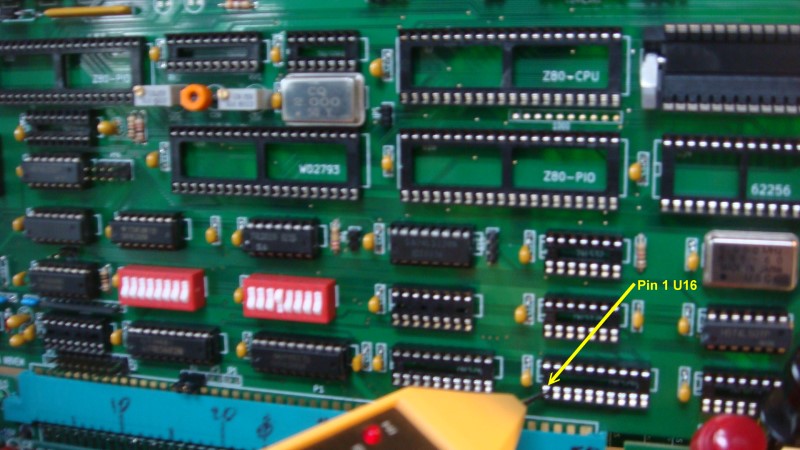
Jump to 0H in RAM. This will have your Z80 continuously input from port 10H. Check with a logic probe pin 12 of U19 pulses low.  Then check that pin 1 of empty socket U16 pulses low .

U20 Check


Next change the above code to:-

D3, 10, C3, 00, 00

Check pin 1 of empty socket U25 pulses low:-

Then change the code to:-

D3, 13, C3, 00, 00

Check that pin 6 of U42 pulses low.

Now go back and insert the code

DB, 10, C3, 00, 00

Insert the Diode D13 (I use a blue LED, initially just hold it in place) and test the code. The diode should light up (if you have it in the right way). Test also:-

D3, 10, C3, 00, 00

If OK, solder the diode in. Make sure ports 11H,12, and 13H do not light up the diode.

Insert U16 & U25 (74LS244's) and U22 (74LS126).

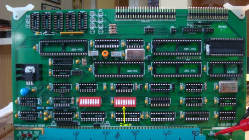
Temporally jumper pin 2 of K15 to ground. Input port 11H.  You should see 10111111B.  Remove the jumper.

You now have the S-100 communication side of the board done!


Next we will insert the Z80 onboard RAM & EEPROM circuitry.

Insert U7  (Z80B), U11 & U10 (Z80B PIO's), U34 (SRAM, HM62256LP), U33 (EEPROM 28C256) and U6 (74LS32).

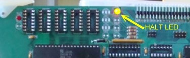
Insert the diode D5 and program an EEPROM with all 76H's (HALT, Z80 opcodes).  Insert and power up the system.  After reset (each time) and a slight delay the LED should light up.   Do not go further until you get this to work. The Z80 must be able to access the onboard EEPROM (at 0H) and see that the first opcode is a HALT (76H) instruction.  Here is what you should see:-

Halt Check  

Before you solder D5 in you can use the two holes to get the orientation of the 4 other LED's nearby. Pick different colors for each LED. Each in position D5 should light up. Then solder all LED into positions (D5, D9, D10 ,D15). For most LED's the longer LED lead goes into the square pad.  Also add LED D16.


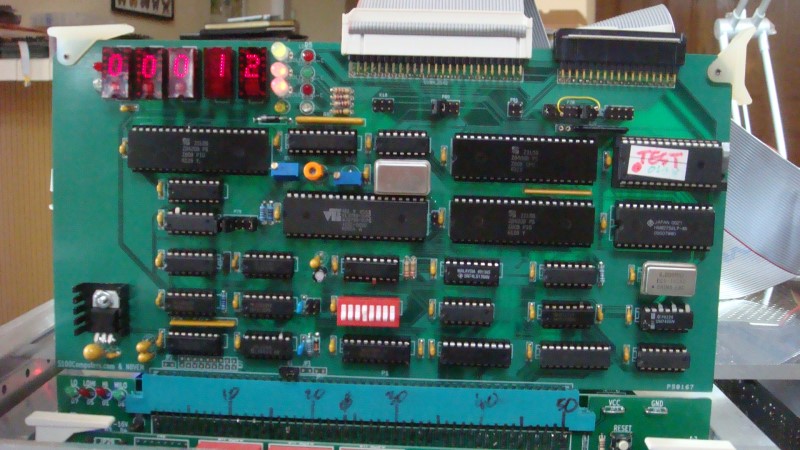
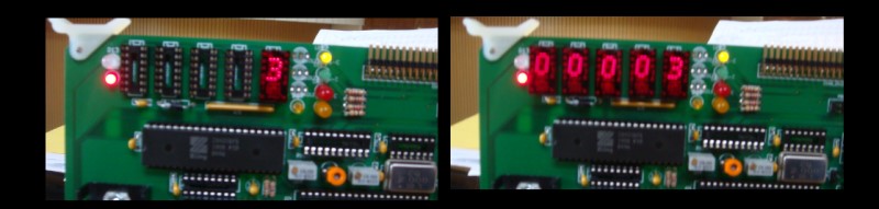
Next insert (only one, they are expensive!)) a TIL 311A HEX LED display in position DIS9. On power up it should display "3".  If it does insert the rest of the TIL's.  Here is a picture of the board so far:-

HEX display Check  


Then download the ZFDC.HEX file software (here) and program an 28C256 EEPROM with it (Note more recent versions of this software may exist in the future. See the bottom of this page).  There are many ways to do this and many programmers available. I particularly like the Wellon VP280. It's Windows 7 compatible and easy to use.  I am currently using ATMEL AT28C256 EEPROMS (from Jameco).

Again power up. This time the HALT LED should NOT light up. The leftmost two HEX displays will continuously count 0 to FFH. The other TIL's should display 0's.  Here is a picture of the board so far:-

After ZFDC Software  

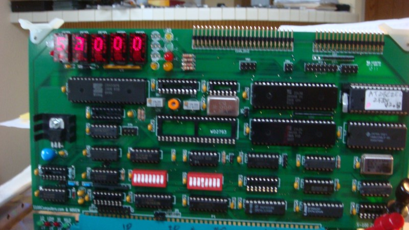
This is the normal startup mode of the board indicating it is ready to be initialized and accept commands from the S-100 system. If you get this far you now have a functional Z80 "computer" working on the board. While you should not need to do so, the HEX display was invaluable for me to initially debug the board. You can put up increasing numbers as you step through your software/hardware development.

Next install all remaining IC's including the WD2793 chip.  Install jumper JP5. 

Again power up your system. You will next need to carefully install the dual color LED's LD1, LD2 and LD3.  Orientate the 3 LED pins so the top LED is red, and the bottom two are green. Carefully solder into place.

The remaining board jumpers are dependent on the size and type of floppy disks you will be using.

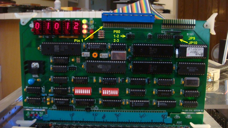
Assume for now we have two 8" drives as A: & B:,  So jumper JP9 1-2 and JP10 1-2.  Jumper P80 1-2 & 2-3.

Connect up the floppy disk ribbon cable connector making sure pin 1 is towards the front of the board on the left hand side

Here is a picture of the completed board.  Note some drives require different jumpers. For example some require jumpers on p79 to start the drive motor. You will need to experiment quite a bit.

Floppy Connections


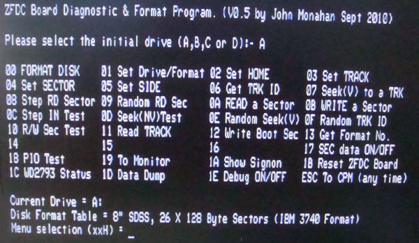
Next launch the S-100/CPM based diagnostic program ZFDCDIAG mentioned above.

Here is it's signon screen:-

Main Menu

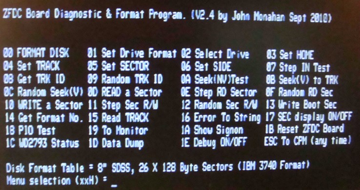
It will come up assuming you are using an 8" disk in drive A: Your first test should be Menu #07. This will repeatedly step the head in one track at a time. It is independent of many disk (and WD2793) parameters. If it does not work, check your drive jumper connections.  Next try Menu #0A.  It should do the same thing. 

If you have drive problems "stepping the head" chances are you do not have either the board jumpers correct or your connections to the drive itself are not configured correctly.  I use a "gerry rigged" jumper shown here to narrow issues like this down with different drives.

Test Connector

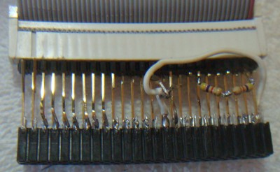
It's not a pretty sight but you only use it when needed. For 8" IBM formatted drives the following pins need to be connected:-

Pins 4 & 14 need to be tied high (to 5V through 470 ohm resistors) and to +5V on the board via a temporary wire jumper.

Pins 18, 22, and 26 are tied to ground.

Pins 20, 34, 36, 38, 40, 42, 44 and 46 are connected to the drive cable.  All other connections are left open. With this "connector" you should be able to step, read and write to the disk is drive A:

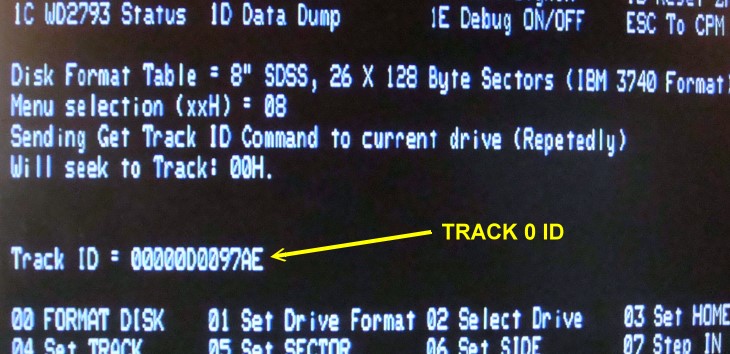
Then assuming you have a formatted disk, try Menu #08.   This will give you the Track ID.  For Track 0 of an 8" Single density disk you will get something like this (depending on the sector the head lands on, see above):-


Track ID


You can then use most of the commands to test your disk/zfdc controller system.  It should work 100% reliable on a properly formatted disk.  Do not even think of using the controller in a CPM system if this is not the case. Also include in the software below is a program to format a disk (8" & 5" disks, most common formats). The is also a simple program to quickly copy one disk to another.


Adjusting the Data Separator setting of the WD2793.
One thing that often scares people away from these early FDC chips is the need to fine tune the data separator/analogue signal of the raw data coming in from the disk.   I have found that the WD2793 works with almost any setting for 8" single density drives. Not so for the double density 5" floppy disks however. Early FDC boards often had elaborate hardware that sometimes required careful adjustment to get a reliable signal, particularly for Double Density modes.  Western Digital greatly simplified this process with the WD2793 chip. All that is required is one 50K  Potentiometer and a 5-50pF variable capacitor.   The adjustment process is as follows:-

Reset the WD2793 chip (Reset on the S-100 system).
Bring up CPM and load the ZFDDIAG program.
Start the boards Monitor program (Menu #19).  

Output 08H to Port 06H (PIO#2B, U11).  Use
QO06,08. This will set the WD chip to double density mode, 8" disk. (LED's should be, from top, Red, Green, Red).

Then Jumper JP 4. This sets the WD2793 "TEST" pin (pin 22) to ground.  (It will not work if JP4 is installed before the above reset).

The with a scope or logic analyzer observe the continuous pulse on pin 29 (TG43).

Adjust the 50K pot on pin 18 (RV1) so the signal on pin 29 has a width of 250ns. It should be the same width as the 2MHz clock pulse on pin 24.

Next adjust the variable capacitor (C29) so that pin 16 has a frequency of 500kHz.  You can use a scope, digital analyzer of simple handheld frequency counter. 

When done be sure to  remove the jumper on pin 22.

The above sounds more complicated than it actually is. In fact I have found if the pot and cap are roughly in the middle of their range the chip works fairly reliable. A poor man's approach might be to do continuous disk sector reads and adjust things on the fly!

Here is a picture of my adjusted board using a USBee logic analyzer.

Signals From Data Seperator

With the above optimization you should be able to read and write sectors to a disk with no errors.  Checkout menu #12 and allow the ZFDC board to randomly read and write sectors for at least 5 minutes.  No errors should be encountered.

Next use the Menu #1 and Menu#0 to change the disk format to a double density disk and format it in that density.   Repeat the above steps. Then try your drive B: and if you have one a 5" drive. 

After you have incorporated the BIOS in your disk operating system thoroughly check things out by copying files from one disk to another (preferably of different densities and sizes). Use the CPM "V" option to check the copy went without errors.

I have written both  banked and non-banked versions of CPM3 for this FDC board. It is extensively written up in the software section of this site. Please click here for more information.

Board Cable Configurations For 8", 5" and 3.5" Drives.
Configuring the board jumpers for 8" drives (A & B) is easy since (with the exception of PerSci Drives) almost all drives have the same ribbon cable pinouts.  In most cases all you need to do is jumper JP9, JP10 and for p80, (1-2 & 2-3).  If the drives HLD does not switch on the drive motor,  jumper p79 (1-2 & 3-4).

Five inch drives unfortunately are more difficult. There are numerous arrangements.  You may need to experiment.
 
Don't worry the cable connecting IC drivers are all OC outputs, so it is difficult to damage anything.  
Here is an example for the once very common TEAC 360K 5" drive:-
  
5 Inch Drive
   
In this case we are using a straight 36 pin ribbon cable (not the twisted IBM PC Floppy cable) The only jumper on the drive itself is D3 (for "Drive Select 3").  Note these drives require a cable termination 330 Ohms resistor pack. It is usually (but not always) soldered into the drive. 

Here is a picture of the jumpers on the ZFDC board:-
  
5 Inch Drive Board Jumpers
   

I typically format 5" disks with this drive in a DSDD CPM86 format as was used on the original IBM-PC.  Select "drive 3" in the ZFDCDIAG software
 
Much has been written on the web about using 3.5" drives in place of 8" drives. See here for example.  As far as the WD2793 chip is concerned it does not "know" (or care) what type of drive it is talking to.  Consequently it is easy to configure the ZFDC board into thinking it is talking to an 8" drive (in terms of S-100 based software) yet the actual physical drive is a silent, small, reliable 3.5" drive (or HD 1.2M 5" drive).  This is because the Western Digital 2793 chip has a frequency divider and can work with 300 or 360RPM drives.

The only issue is, there is no agreed upon standard disk format for CPM for these high capacity drives   I have found that the ZFDC board will work with any 8" disk format on a physical 3.5" drive (or HD 5" drive), completely transparently -- even the Morrow 1K double sided, double density 8" formats. However there is a lot of wasted unused space.   I normally use these drives formatted in the formats used by the IBM-PC/MSDOS systems.

 
1    IBM 5" HD drives.    1.2M Capacity, Double density, double sided, 512 byte sectors, 16 sectors/track, 80 tracks
 2    IBM 3.5"  drives.      1,44M Capacity Double density, double sided, 512 byte sectors, 18 sectors/track, 80 tracks


These formats utilize the disk to their full capacity.

Both the ZFDCDIAG and ZFORMAT software (see below) have menu options to format these drives as CPM drives where all the sectors are simply filled with E5's or as MSDOS/Windows compatable disks in the above formats. In the case of MSDOS disks the software takes care of the post formatting 'initilization' of the boot and FAT sectors that MSDOS/Windows requires to see these disks as valid formatted empty disks.  This involves filling the sectors with 0's , writing 28 bytes of data in the first sector and configuring the two FAT tables on a disk.  With this done you can pop either disk in a Windows machine and write on it.  Of course the data will not be much use to you if you are running CPM.  This whole process however will become very relevent when we bring up our S-100 8086 family of S-100 boards.

 
Here is a picture of a 3.5" drive, (a TEAC FD-235HF), configured as the third drive (Drive D: in CPM).  As far as CPM is concerned it is just another 8" drive with 512 byte sectors (18/track, doubel sided, 80 tracks).  For 3.5" drives I use the common IBM-PC floppy cables that have the twisted section for its drive A: for these 1.44M drives. These are very common these days. In the example below I use the fancy non-ribbon type for only one floppy.

Floppy Connections 2

If you decide to use this cable for a 3.5" drive on the boards drive D:  Jumper JP12. Jumper P79 7-8, for  P78  1-2, 13 to 12  & 8.

Source of chips
Most of the IC's use on this board are common 74LSxx chips available from numerous sources such a Jameco, Mouser & DigiKey.  Note the 1K resistor R51 should be 1% accuracy. The WD2793 is not too common. It was used in some old Atari systems. They can from time to time be found on eBay.  A great source of older chips like this  is Unicorn Electronics who have very reasonable prices - though chips are hard to find on their web site. The WD2793 can also be obtained locally here in the San Francisco bay area at Anchor Electronics. They take phone orders as well and also stock the high speed "B" versions of the Zilog chips. 

The TIL 311A's are expensive (~$20 each from places like Jameco).  However overseas outfits like Utsource sell them in small quantities for ~$5 each. Utsource have about a 1 week delivery time to the US since they use DHL.  It is indeed frustrating these LED HEX displays are so expensive. With the exception of the even rarer HP-5082's other such displays display only the digits 0-9.  An alternative approach would be to use a 7 segment LED decoder such as a DM9368 and a simple 7 segment LED display. However these too are no longer normally stocked.  Normal single line flat panel LCD displays just do not show up well when the card is in the S-100 bus card cage.

     
The links below will contain the most recent schematic for this board.
Note, it may change over time and some IC part or pin numbers may not correlate exactly with the text in the article above.

MOST CURRENT ZFDC BOARD SCHEMATIC (V3 FINAL, 4/19/2011)
MOST CURRENT ZFDC BOARD LAYOUT  (V3 FINAL, 4/19/2011)
MOST CURRENT ZFDC.Z80  (V2.9    5/1//2011)
MOST CURRENT ZFDCDIAG.Z80  (VV2.9   5/1/2011)
MOST CURRENT ZFDCFORM.Z80   (V1.3    5/1/2011)
MOST CURRENT SOURCE CODE FOR ABOVE FILES    (5/6/2011)

Other pages describing my S-100 hardware and software.
Please click here to continue...

This page was last modified on 09/18/2011